From WikiChip
Editing hisilicon/kirin/970
Warning: You are not logged in. Your IP address will be publicly visible if you make any edits. If you log in or create an account, your edits will be attributed to your username, along with other benefits.
The edit can be undone.
Please check the comparison below to verify that this is what you want to do, and then save the changes below to finish undoing the edit.
This page supports semantic in-text annotations (e.g. "[[Is specified as::World Heritage Site]]") to build structured and queryable content provided by Semantic MediaWiki. For a comprehensive description on how to use annotations or the #ask parser function, please have a look at the getting started, in-text annotation, or inline queries help pages.
| Latest revision | Your text | ||
| Line 145: | Line 145: | ||
== Neural Network Processing Unit (NPU) == | == Neural Network Processing Unit (NPU) == | ||
[[File:kirin 970 npu.png|right|350px]] | [[File:kirin 970 npu.png|right|350px]] | ||
| − | The Kirin 970 incorporates a new [[neural processor|Neural Network Processing Unit]] (NPU) designed specifically to be used as an AI accelerator. According to CEO Richard Yu, who also introduced the processor at 2017 IFA, the NPU uses up the die area of roughly half of the CPU while consuming 50% less power and performing around 25 times faster than a traditional CPU for tasks such as photo recognition. The NPU is said to deliver 1.92 [[TFLOP]]s (HP 16-bit) | + | The Kirin 970 incorporates a new [[neural processor|Neural Network Processing Unit]] (NPU) designed specifically to be used as an AI accelerator. According to CEO Richard Yu, who also introduced the processor at 2017 IFA, the NPU uses up the die area of roughly half of the CPU while consuming 50% less power and performing around 25 times faster than a traditional CPU for tasks such as photo recognition. The NPU is said to deliver 1.92 [[TFLOP]]s (HP 16-bit). While the exact architectural details of the NPU have been withheld, the NPU appear to be a licensed IP design from [[Cambricon Technologies]]. |
== Utilizing devices == | == Utilizing devices == | ||
Facts about "Kirin 970 - HiSilicon"
| base frequency | 1,800 MHz (1.8 GHz, 1,800,000 kHz) + and 2,360 MHz (2.36 GHz, 2,360,000 kHz) + |
| core count | 8 + |
| core name | Cortex-A53 + and Cortex-A73 + |
| designer | HiSilicon + and ARM Holdings + |
| die area | 96.72 mm² (0.15 in², 0.967 cm², 96,720,000 µm²) + |
| die length | 9.75 mm (0.975 cm, 0.384 in, 9,750 µm) + |
| die width | 9.92 mm (0.992 cm, 0.391 in, 9,920 µm) + |
| family | Kirin + |
| first announced | September 1, 2017 + |
| first launched | September 1, 2017 + |
| full page name | hisilicon/kirin/970 + |
| has ecc memory support | false + |
| instance of | microprocessor + |
| integrated gpu | Mali-G72 + |
| integrated gpu base frequency | 746 MHz (0.746 GHz, 746,000 KHz) + |
| integrated gpu designer | ARM Holdings + |
| integrated gpu execution units | 12 + |
| isa | ARMv8 + |
| isa family | ARM + |
| l1$ size | 256 KiB (262,144 B, 0.25 MiB) + and 512 KiB (524,288 B, 0.5 MiB) + |
| l1d$ size | 128 KiB (131,072 B, 0.125 MiB) + and 256 KiB (262,144 B, 0.25 MiB) + |
| l1i$ size | 128 KiB (131,072 B, 0.125 MiB) + and 256 KiB (262,144 B, 0.25 MiB) + |
| l2$ size | 1 MiB (1,024 KiB, 1,048,576 B, 9.765625e-4 GiB) + and 2 MiB (2,048 KiB, 2,097,152 B, 0.00195 GiB) + |
| ldate | September 1, 2017 + |
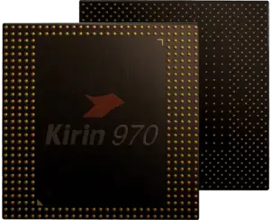
| main image |  + + |
| manufacturer | TSMC + |
| market segment | Mobile + |
| max cpu count | 1 + |
| max memory | 8,192 MiB (8,388,608 KiB, 8,589,934,592 B, 8 GiB, 0.00781 TiB) + |
| max memory bandwidth | 27.82 GiB/s (28,487.68 MiB/s, 29.871 GB/s, 29,871.498 MB/s, 0.0272 TiB/s, 0.0299 TB/s) + |
| max memory channels | 4 + |
| microarchitecture | Cortex-A53 + and Cortex-A73 + |
| model number | 970 + |
| name | Kirin 970 + |
| part number | Hi3670 + |
| process | 10 nm (0.01 μm, 1.0e-5 mm) + |
| series | 900 + |
| smp max ways | 1 + |
| supported memory type | LPDDR4X-3732 + |
| technology | CMOS + |
| thread count | 8 + |
| transistor count | 5,500,000,000 + |
| used by | Huawei Mate 10 +, Huawei Mate 10 Pro +, Huawei Mate 10 Porsche Design +, Huawei P20 +, Huawei Mate RS Porsche Design +, Honor 10 +, Huawei Nova 3 +, Honor V10 (Honor View 10) +, Honor Note 10 +, Huawei P20 Pro +, Huawei Nova 4 +, HiKey 970 +, Honor 8 Pro +, Honor Play 2 + and Honor Play + |
| word size | 64 bit (8 octets, 16 nibbles) + |