From WikiChip
Difference between revisions of "intel/core i5/i5-8350u"
| (5 intermediate revisions by 2 users not shown) | |||
| Line 1: | Line 1: | ||
{{intel title|Core i5-8350U}} | {{intel title|Core i5-8350U}} | ||
| − | {{ | + | {{chip |
|future=Yes | |future=Yes | ||
|name=Core i5-8350U | |name=Core i5-8350U | ||
| Line 19: | Line 19: | ||
|frequency=1,700 MHz | |frequency=1,700 MHz | ||
|turbo frequency1=3,600 MHz | |turbo frequency1=3,600 MHz | ||
| + | |turbo frequency2=3,600 MHz | ||
| + | |turbo frequency3=3,600 MHz | ||
| + | |turbo frequency4=3,600 MHz | ||
|bus type=OPI | |bus type=OPI | ||
|bus rate=4 GT/s | |bus rate=4 GT/s | ||
| Line 32: | Line 35: | ||
|process=14 nm | |process=14 nm | ||
|technology=CMOS | |technology=CMOS | ||
| + | |die area=123 mm² | ||
|word size=64 bit | |word size=64 bit | ||
|core count=4 | |core count=4 | ||
| Line 50: | Line 54: | ||
|package module 1={{packages/intel/fcbga-1356}} | |package module 1={{packages/intel/fcbga-1356}} | ||
}} | }} | ||
| − | '''Core i5-8350U''' is a {{arch|64}} [[quad-core]] performance [[x86]] mobile microprocessor introduced by [[Intel]] in mid-[[2017]]. This processor, which is based on an enhanced version of the {{intel|Kaby Lake|l=arch}} microarchitecture, is manufactured on Intel's 2nd generation enhanced [[14 nm process|14nm+ process]]. The i5-8350U operates at 1.7 GHz with a TDP of 15 W and {{intel|Turbo Boost}} frequency of up to 3.6 GHz. This MPU supports up to 32 GiB of dual-channel DDR4-2400 memory and incorporates Intel's {{intel| | + | '''Core i5-8350U''' is a {{arch|64}} [[quad-core]] performance [[x86]] mobile microprocessor introduced by [[Intel]] in mid-[[2017]]. This processor, which is based on an enhanced version of the {{intel|Kaby Lake|l=arch}} microarchitecture, is manufactured on Intel's 2nd generation enhanced [[14 nm process|14nm+ process]]. The i5-8350U operates at 1.7 GHz with a TDP of 15 W and {{intel|Turbo Boost}} frequency of up to 3.6 GHz. This MPU supports up to 32 GiB of dual-channel DDR4-2400 memory and incorporates Intel's {{intel|UHD Graphics 620}} [[IGP]] operating at 300 MHz with a burst frequency of 1.15 GHz. |
| + | |||
| + | This model has a configurable TDP-down of 10 W at 800 MHz and a TDP-up of 25 W at 1.9 GHz. | ||
== Cache == | == Cache == | ||
| Line 102: | Line 108: | ||
== Graphics == | == Graphics == | ||
{{integrated graphics | {{integrated graphics | ||
| − | | gpu = | + | | gpu = UHD Graphics 620 |
| device id = 0x5917 | | device id = 0x5917 | ||
| designer = Intel | | designer = Intel | ||
| Line 246: | Line 252: | ||
* [[14 nm process|14 nm+ process]] | * [[14 nm process|14 nm+ process]] | ||
* 11 metal layers | * 11 metal layers | ||
| + | * 123 mm² die size | ||
* 4 CPU cores + 24 GPU EUs | * 4 CPU cores + 24 GPU EUs | ||
Latest revision as of 16:39, 23 November 2018
| Edit Values | |||||||||||||
| Core i5-8350U | |||||||||||||
 | |||||||||||||
| General Info | |||||||||||||
| Designer | Intel | ||||||||||||
| Manufacturer | Intel | ||||||||||||
| Model Number | i5-8350U | ||||||||||||
| Part Number | FJ8067703282016 | ||||||||||||
| S-Spec | SR3L9 | ||||||||||||
| Market | Mobile | ||||||||||||
| Introduction | August 21, 2017 (announced) August 21, 2017 (launched) | ||||||||||||
| Release Price | $297.00 | ||||||||||||
| Shop | Amazon | ||||||||||||
| General Specs | |||||||||||||
| Family | Core i5 | ||||||||||||
| Series | i5-8000 | ||||||||||||
| Locked | Yes | ||||||||||||
| Frequency | 1,700 MHz | ||||||||||||
| Turbo Frequency | 3,600 MHz (1 core), 3,600 MHz (2 cores), 3,600 MHz (3 cores), 3,600 MHz (4 cores) | ||||||||||||
| Bus type | OPI | ||||||||||||
| Bus rate | 4 GT/s | ||||||||||||
| Clock multiplier | 17 | ||||||||||||
| Microarchitecture | |||||||||||||
| ISA | x86-64 (x86) | ||||||||||||
| Microarchitecture | Kaby Lake | ||||||||||||
| Platform | Kaby Lake | ||||||||||||
| Core Name | Kaby Lake R | ||||||||||||
| Core Family | 6 | ||||||||||||
| Core Model | 142 | ||||||||||||
| Core Stepping | Y0 | ||||||||||||
| Process | 14 nm | ||||||||||||
| Technology | CMOS | ||||||||||||
| Die | 123 mm² | ||||||||||||
| Word Size | 64 bit | ||||||||||||
| Cores | 4 | ||||||||||||
| Threads | 8 | ||||||||||||
| Max Memory | 32 GiB | ||||||||||||
| Multiprocessing | |||||||||||||
| Max SMP | 1-Way (Uniprocessor) | ||||||||||||
| Electrical | |||||||||||||
| Vcore | 0.55 V-1.52 V | ||||||||||||
| TDP | 15 W | ||||||||||||
| cTDP down | 10 W | ||||||||||||
| cTDP down frequency | 800 MHz | ||||||||||||
| cTDP up | 25 W | ||||||||||||
| cTDP up frequency | 1,900 MHz | ||||||||||||
| Tjunction | 0 °C – 100 °C | ||||||||||||
| Tstorage | -25 °C – 125 °C | ||||||||||||
| Packaging | |||||||||||||
| |||||||||||||
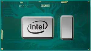
Core i5-8350U is a 64-bit quad-core performance x86 mobile microprocessor introduced by Intel in mid-2017. This processor, which is based on an enhanced version of the Kaby Lake microarchitecture, is manufactured on Intel's 2nd generation enhanced 14nm+ process. The i5-8350U operates at 1.7 GHz with a TDP of 15 W and Turbo Boost frequency of up to 3.6 GHz. This MPU supports up to 32 GiB of dual-channel DDR4-2400 memory and incorporates Intel's UHD Graphics 620 IGP operating at 300 MHz with a burst frequency of 1.15 GHz.
This model has a configurable TDP-down of 10 W at 800 MHz and a TDP-up of 25 W at 1.9 GHz.
Cache[edit]
- Main article: Kaby Lake § Cache
|
Cache Organization
Cache is a hardware component containing a relatively small and extremely fast memory designed to speed up the performance of a CPU by preparing ahead of time the data it needs to read from a relatively slower medium such as main memory. The organization and amount of cache can have a large impact on the performance, power consumption, die size, and consequently cost of the IC. Cache is specified by its size, number of sets, associativity, block size, sub-block size, and fetch and write-back policies. Note: All units are in kibibytes and mebibytes. |
|||||||||||||||||||||||||||||||||||||
|
|||||||||||||||||||||||||||||||||||||
Memory controller[edit]
|
Integrated Memory Controller
|
||||||||||||||
|
||||||||||||||
Expansions[edit]
Expansion Options |
|||||
|
|||||
Graphics[edit]
|
Integrated Graphics Information
|
||||||||||||||||||||||||||||||||||||||||||||||||||||||||||||||||||||
|
||||||||||||||||||||||||||||||||||||||||||||||||||||||||||||||||||||
| [Edit] Kaby Lake (Gen9.5) Hardware Accelerated Video Capabilities | |||||||
|---|---|---|---|---|---|---|---|
| Codec | Encode | Decode | |||||
| Profiles | Levels | Max Resolution | Profiles | Levels | Max Resolution | ||
| MPEG-2 (H.262) | Main | High | 1080p (FHD) | Main | Main, High | 1080p (FHD) | |
| MPEG-4 AVC (H.264) | High, Main | 5.1 | 2160p (4K) | Main, High, MVC, Stereo | 5.1 | 2160p (4K) | |
| JPEG/MJPEG | Baseline | - | 16k x 16k | Baseline | Unified | 16k x 16k | |
| HEVC (H.265) | Main, Main 10 | 5.1 | 2160p (4K) | Main, Main 10 | 5.1 | 2160p (4K) | |
| VC-1 | ✘ | Advanced, Main, Simple | 3, High, Simple | 3840x3840 | |||
| VP8 | Unified | Unified | N/A | 0 | Unified | 1080p | |
| VP9 | 0 | 2160p (4K) | 0, 2 | Unified | 2160p (4K) | ||
Features[edit]
[Edit/Modify Supported Features]
Die Shot[edit]
- See also: Kaby Lake § Die Shot
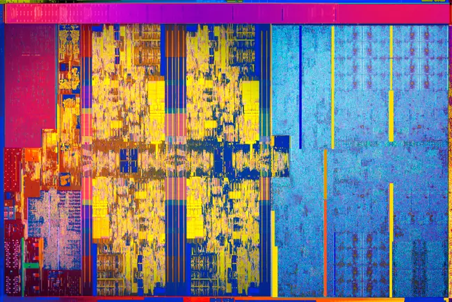
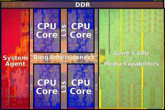
A die shot of Intel's Kaby Lake R Quad Core mobile processors:
- 14 nm+ process
- 11 metal layers
- 123 mm² die size
- 4 CPU cores + 24 GPU EUs
Facts about "Core i5-8350U - Intel"
| Has subobject "Has subobject" is a predefined property representing a container construct and is provided by Semantic MediaWiki. | Core i5-8350U - Intel#package + and Core i5-8350U - Intel#pcie + |
| base frequency | 1,700 MHz (1.7 GHz, 1,700,000 kHz) + |
| bus rate | 4,000 MT/s (4 GT/s, 4,000,000 kT/s) + |
| bus type | OPI + |
| clock multiplier | 17 + |
| core count | 4 + |
| core family | 6 + |
| core model | 142 + |
| core name | Kaby Lake R + |
| core stepping | Y0 + |
| core voltage (max) | 1.52 V (15.2 dV, 152 cV, 1,520 mV) + |
| core voltage (min) | 0.55 V (5.5 dV, 55 cV, 550 mV) + |
| designer | Intel + |
| device id | 0x5917 + |
| die area | 123 mm² (0.191 in², 1.23 cm², 123,000,000 µm²) + |
| family | Core i5 + |
| first announced | August 21, 2017 + |
| first launched | August 21, 2017 + |
| full page name | intel/core i5/i5-8350u + |
| has advanced vector extensions | true + |
| has advanced vector extensions 2 | true + |
| has ecc memory support | false + |
| has extended page tables support | true + |
| has feature | Advanced Vector Extensions +, Advanced Vector Extensions 2 +, Advanced Encryption Standard Instruction Set Extension +, Hyper-Threading Technology +, Turbo Boost Technology 2.0 +, Enhanced SpeedStep Technology +, Speed Shift Technology +, Intel VT-x +, Intel VT-d +, Extended Page Tables +, Memory Protection Extensions +, Software Guard Extensions +, Secure Key Technology +, OS Guard +, Flex Memory Access +, Smart Response Technology +, My WiFi Technology + and Identity Protection Technology + |
| has intel enhanced speedstep technology | true + |
| has intel flex memory access support | true + |
| has intel identity protection technology support | true + |
| has intel my wifi technology support | true + |
| has intel secure key technology | true + |
| has intel smart response technology support | true + |
| has intel speed shift technology | true + |
| has intel supervisor mode execution protection | true + |
| has intel turbo boost technology 2 0 | true + |
| has intel vt-d technology | true + |
| has intel vt-x technology | true + |
| has locked clock multiplier | true + |
| has second level address translation support | true + |
| has simultaneous multithreading | true + |
| has x86 advanced encryption standard instruction set extension | true + |
| instance of | microprocessor + |
| integrated gpu | UHD Graphics 620 + |
| integrated gpu base frequency | 300 MHz (0.3 GHz, 300,000 KHz) + |
| integrated gpu designer | Intel + |
| integrated gpu execution units | 24 + |
| integrated gpu max frequency | 1,100 MHz (1.1 GHz, 1,100,000 KHz) + |
| integrated gpu max memory | 32,768 MiB (33,554,432 KiB, 34,359,738,368 B, 32 GiB) + |
| isa | x86-64 + |
| isa family | x86 + |
| l1$ size | 256 KiB (262,144 B, 0.25 MiB) + |
| l1d$ description | 8-way set associative + |
| l1d$ size | 128 KiB (131,072 B, 0.125 MiB) + |
| l1i$ description | 8-way set associative + |
| l1i$ size | 128 KiB (131,072 B, 0.125 MiB) + |
| l2$ description | 4-way set associative + |
| l2$ size | 1 MiB (1,024 KiB, 1,048,576 B, 9.765625e-4 GiB) + |
| l3$ description | 12-way set associative + |
| l3$ size | 6 MiB (6,144 KiB, 6,291,456 B, 0.00586 GiB) + |
| ldate | 3000 + |
| main image |  + + |
| manufacturer | Intel + |
| market segment | Mobile + |
| max cpu count | 1 + |
| max junction temperature | 373.15 K (100 °C, 212 °F, 671.67 °R) + |
| max memory | 32,768 MiB (33,554,432 KiB, 34,359,738,368 B, 32 GiB, 0.0313 TiB) + |
| max memory bandwidth | 35.76 GiB/s (36,618.24 MiB/s, 38.397 GB/s, 38,397.008 MB/s, 0.0349 TiB/s, 0.0384 TB/s) + |
| max memory channels | 2 + |
| max storage temperature | 398.15 K (125 °C, 257 °F, 716.67 °R) + |
| microarchitecture | Kaby Lake + |
| min junction temperature | 273.15 K (0 °C, 32 °F, 491.67 °R) + |
| min storage temperature | 248.15 K (-25 °C, -13 °F, 446.67 °R) + |
| model number | i5-8350U + |
| name | Core i5-8350U + |
| package | FCBGA-1356 + |
| part number | FJ8067703282016 + |
| platform | Kaby Lake + |
| process | 14 nm (0.014 μm, 1.4e-5 mm) + |
| release price | $ 297.00 (€ 267.30, £ 240.57, ¥ 30,689.01) + |
| s-spec | SR3L9 + |
| series | i5-8000 + |
| smp max ways | 1 + |
| supported memory type | DDR4-2400 + and LPDDR3-2133 + |
| tdp | 15 W (15,000 mW, 0.0201 hp, 0.015 kW) + |
| tdp down | 10 W (10,000 mW, 0.0134 hp, 0.01 kW) + |
| tdp down frequency | 800 MHz (0.8 GHz, 800,000 kHz) + |
| tdp up | 25 W (25,000 mW, 0.0335 hp, 0.025 kW) + |
| tdp up frequency | 1,900 MHz (1.9 GHz, 1,900,000 kHz) + |
| technology | CMOS + |
| thread count | 8 + |
| turbo frequency (1 core) | 3,600 MHz (3.6 GHz, 3,600,000 kHz) + |
| turbo frequency (2 cores) | 3,600 MHz (3.6 GHz, 3,600,000 kHz) + |
| turbo frequency (3 cores) | 3,600 MHz (3.6 GHz, 3,600,000 kHz) + |
| turbo frequency (4 cores) | 3,600 MHz (3.6 GHz, 3,600,000 kHz) + |
| word size | 64 bit (8 octets, 16 nibbles) + |
| x86/has memory protection extensions | true + |
| x86/has software guard extensions | true + |

