(→NCORE NPU) |
(→CNS Core) |
||
| Line 21: | Line 21: | ||
:[[File:cha soc block diagram.svg|450px]] | :[[File:cha soc block diagram.svg|450px]] | ||
==== CNS Core ==== | ==== CNS Core ==== | ||
| − | :[[File:cns block diagram.svg| | + | :[[File:cns block diagram.svg|750px]] |
| + | |||
==== NCORE NPU ==== | ==== NCORE NPU ==== | ||
:[[File:ncore block diagram.svg|700px]] | :[[File:ncore block diagram.svg|700px]] | ||
Revision as of 16:14, 23 January 2020
| Edit Values | |
| CHA µarch | |
| General Info | |
| Arch Type | CPU |
| Designer | Centaur Technology |
| Manufacturer | TSMC |
| Process | 16 nm |
| Core Configs | 8 |
| Instructions | |
| ISA | x86-64 |
CHA is a 16-nanometer x86 SoC microarchitecture designed by Centaur Technology for the server market.
Contents
Process technology
| This section is empty; you can help add the missing info by editing this page. |
Architecture
Key changes from CN
| This section is empty; you can help add the missing info by editing this page. |
Block Diagram
CHA SoC
CNS Core
NCORE NPU
Memory Hierarchy
- Cache
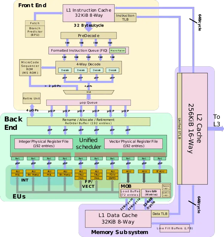
- L1I Cache:
- 32 KiB, 8-way set associative
- 64 sets, 64 B line size
- 64 B/cycle bandwidth to L1$
- 32 KiB, 8-way set associative
- L1D Cache:
- 32 KiB, 8-way set associative
- 64 sets, 64 B line size
- 64 B/cycle load bandwidth
- 32 B/cycle store bandwidth
- 64 B/cycle bandwidth to L1$
- 32 KiB, 8-way set associative
- L2 Cache:
- Unified, 256 KiB, 16-way set associative
- 256 sets, 64 B line size
- 64 B/cycle bandwidth to L1$
- Unified, 256 KiB, 16-way set associative
- L3 Cache/LLC:
- 2 MiB Per core, shared across all cores
- Up to 16-way set associative
- 64 B line size
- Per each core:
- Read: 32 B/cycle (@ ring clock)
- Write: 32 B/cycle (@ ring clock)
- System DRAM:
- 8 B/cycle/channel (@ memory clock)
- 4 Channels
- DDR4, up to 3,200 MT/s
- L1I Cache:
Overview
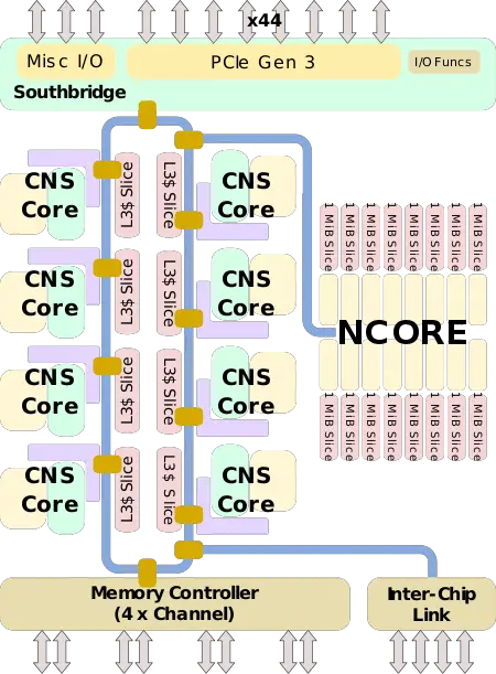
CHA is an x86 SoC designed by Centaur for the server, edge, and AI market. Fabricated on TSMC 16 nm process, the chip integrates 8 new high-performance x86 "CNS" cores interconnected on a ring along with a high-performance "NCORE" neural processor. This chip is the first server x86 chip to integrate an AI accelerator right on-die and is designed to reduce the dependency on AI acceleration through additional hardware in order to simplify the platform and cost. The new CNS cores also introduce the AVX-512 extension in order to offer better performance and more flexibility.
The CHA SoC incorporates both the source bridge and north bridge on-die. The chip supports for up to quad-channel DDR4 memory and up to 44 PCIe Gen 3 lanes. Additionally, CHA supports the ability to directly link to a second CHA SoC in a 2-way multiprocessing configuration.
Ring
CHA interlinks all the components on the chip through a bidirectional ring interconnect. There is a dedicated ring stop for every one of the eight CNS cores connected at the L3 cache slice, one for the NCORE NPU, one for the southbridge, and another one for the memory controller.
The ring itself consists of two opposing unidirectional rings. Each ring is 512-bit wide. Each cycle, data is passed from one ring stop to the next ring stop. The ring operates at the same clock frequency as the cores. At 2.5 GHz, the ring has a peak theoretical bidirectional bandwidth of 2.56 Tb/s or 320 GB/s.
CNS Core
| This section is empty; you can help add the missing info by editing this page. |
NCORE NPU
The AI accelerator coprocessor sits on the same ring as the rest of the chip with its own dedicated ring stop. NCORE has two DMA channels, capable of reading and writing to/from the L3 cache slices, DRAM, and in theory also I/O. NCORE has a relatively different architecture to many of the dedicated neural processors developed by various startups. To that end, NCORE is an extremely-wide 32,768-bit VLIW SIMD coprocessor. The coprocessor is a programmable coprocessor that's capable of controlling up to 4K-lanes of logic each cycle at the same clock frequency as the CPU cores. 4K bytes operations are available every cycle and since the NCORE is directly connected to the ring, latency is extremely low compared to externally-attached accelerators.
Instructions are brought to the NCORE through the ring and are stored in a centralized instruction unit. The unit incorporates a 12 KiB instruction cache and a 4 KiB instruction ROM. Each cycle, a single 128-bit instruction is fetched, decoded, and gets executed by a sequencer which controls simultaneously all the compute slices and memory. The instruction ROM is used for executing validation code as well as commonly-used functions. The instruction sequencer incorporates a loop counter and various special registers along with sixteen address registers and dedicated hardware for performing on various addressing modes and auto-incrementation operations. The entire NCORE datapath is 4,096-byte wide.
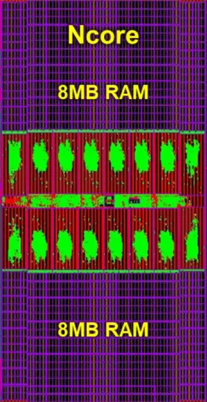
Data to the NCORE are fed into the NCORE caches. Data is fed by the two DMA channels on the ring stop interface. These DMA channels can go out to the other caches or memory asynchronously. On occasion, data may be fed from the device driver or software running on one of the CPU cores which can move instructions and data into the NCORE RAM. The NCORE features a very large and very fast 16 MiB SRAM cache. The cache comprises two SRAM banks - D-RAM and W-RAM - each one is 4,096-bytes wide and is 64-bit ECC-protected. The two SRAMs operate at the same clock as the NCORE itself which is the same clock as the CPU cores. Each cycle, up to two reads (one form each bank) can be done. With each one being 4,096-byte interface, each cycle up to 8,192-bytes can be read into the compute interface. This enables the NCORE to have a theoretical peak read bandwidth of 20.5 TB/s. It's worth noting that physically, the NCORE is built up using small compute units called "slices" or "neurons". The design is done in this way in order to allow for future reconfigurability. The full CHA configuration features 16 slices. Each slice is a 256-byte wide SIMD unit and is accompanied by its own 2,048 256B-wide rows cache slice.
The compute interface passes the data from the RAMs to the neural data unit. The neural data unit operates on incoming data on each clock before it goes to the SIMD processing unit. The purpose of the data unit is to simply prepare data for the neural processing unit by doing various pre-processing. The data unit has a four-entry 4K register file which can also serve as inputs for various operations and has output to the next stage in the pipeline. The data unit can do operations such as rotate on the entire 4K-byte line, broadcast (taking one byte from each 64B-slice and expend it into 64 bytes for replication used in weight structuring for convolutions), merge from two inputs (e.g., RAM and register), compress data (for pooling operations), and various other specialized functions.
Each cycle, the neural processing unit reads data out of one or two of the four registers in the neural data unit. The neural processing unit does various computations such as MAC operations, shifting, min/max, and various other functions designed to add flexibility in terms of support in preparation for future AI functionalities and operations. The neural processing unit incorporates a 32-bit 4K accumulator which can operate in both 32b-integer and 32b-floating-point modes. The accumulator saturates on overflows to prevent wrap-around (e.g., the biggest positive to biggest negative). Following the millions or billions of repeated MAC operations, the output is sent to the output unit for post-processing.
Data from the neural processing unit is sent to the output unit for post-processing. Here the unit incorporates an activation unit which can perform the standard activation functions such as sigmoid, TanH, ReLu, and others. Additionally, the output unit can perform data compression and quantization to be used in the next convolution. The output unit incorporates various other less common functionalities that run at a slightly slower rate than 4K/clock. Finally, data is written back to one of the memory banks each cycle.
On various rare occasions, some functionality might not be possible on the NCORE (e.g., an operation that's done once an image). Here, the core can use the standard x86 core to do such operations. Centaur's device driver manages the runtime stack which is capable of feeding the NCORE with NCORE instructions and operations and the x86 core with various other subroutines to execute when necessary which can take advantage of the AVX-512 support to accelerate various operations.
Die
SoC
- TSMC 16 nm process
- 195 mm²
Core group
NCORE
- 32,768-bits SIMD, 16 MiB cache
- 34.4 mm² silicon area
Bibliography
- Centaur. personal communication. November 2019.
See also
- Direct Competition
| codename | CHA + |
| core count | 8 + |
| designer | Centaur Technology + |
| full page name | centaur/microarchitectures/cha + |
| instance of | microarchitecture + |
| instruction set architecture | x86-64 + |
| manufacturer | TSMC + |
| microarchitecture type | CPU + |
| name | CHA + |
| process | 16 nm (0.016 μm, 1.6e-5 mm) + |


